(China (Mainland))

Product Summary
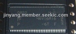
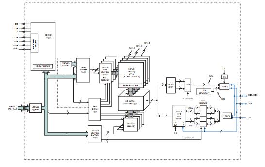
The MT46V16M16P-6T:F is a Double Data Rate (DDR) SDRAM. It uses a double data rate architecture to achieve high-speed operation. A single read or write access for the MT46V16M16P-6T:F effectively consists of a single 2n-bit-wide, one-clock-cycle data transfer at the internal DRAM core and two corresponding n-bit-wide, one-half-clock-cycle data transfers at the I/O pins. The MT46V16M16P-6T:F provides for programmable READ or WRITE burst lengths of 2, 4, or 8 locations.
Parametrics
MT46V16M16P-6T:F absolute maximum ratings: (1)VDD supply voltage relative to VSS:–1V to +3.6V; (2)VDDQ supply voltage relative to VSS:–1V to +3.6V; (3)VREF and inputs voltage relative to VSS:–1V to +3.6V; (4)I/O pins voltage relative to VSS:–0.5V to VDDQ + 0.5V; (5)Storage temperature (plastic):–55℃ to +150℃; (6)Short circuit output current:50mA.
Features
MT46V16M16P-6T:F features: (1)Bidirectional data strobe (DQS) transmitted/received with data, that is, source-synchronous data capture (x16 has two - one per byte); (2)Internal, pipelined double-data-rate (DDR) architecture; two data accesses per clock cycle; (3)Differential clock inputs (CK and CK#); (4)Commands entered on each positive CK edge; (5)DQS edge-aligned with data for READs; centeraligned with data for WRITEs; (6)DLL to align DQ and DQS transitions with CK; (7)Four internal banks for concurrent operation; (8)Data mask (DM) for masking write data (x16 has two - one per byte); (9)Programmable burst lengths (BL): 2, 4, or 8; (10)Auto refresh ; (11)Longer-lead TSOP for improved reliability (OCPL); (12)2.5V I/O (SSTL_2-compatible); (13)Concurrent auto precharge option supported; (14)tRAS lockout supported (tRAP = tRCD).
Diagrams
| Image | Part No | Mfg | Description |  |
Pricing (USD) |
Quantity | ||||
|---|---|---|---|---|---|---|---|---|---|---|
 |
 MT46V16M16P-6T:F |
|
IC DDR SDRAM 256MBIT 6NS 66TSOP |
Data Sheet |
Negotiable |
|
||||
|
MT46V16M16P-6T:F TR |
|
IC DDR SDRAM 256MBIT 6NS 66TSOP |
Data Sheet |
Negotiable |
|
||||